
Key Takeaways
- PCB manufacturers, including WellPCB, routinely manage panelization to streamline production and ensure manufacturing compatibility for both prototypes and large-scale orders.
- Designers can provide single-board layouts or pre-panelized files; however, manufacturers often optimize or create custom panelization based on equipment, order size, and assembly requirements.
- Effective communication between clients and manufacturers regarding panel dimensions, assembly constraints, and special needs is essential for successful panelization and smooth production processes.
- Standard panelization practices include using V-scoring, tab-routing, proper fiducial placement, and following IPC standards to maximize yield, reduce waste, and facilitate automated assembly.
- Reviewing and approving digital panel proofs, as well as heeding manufacturer feedback, helps prevent errors and ensures the final panels meet both design and assembly specifications.
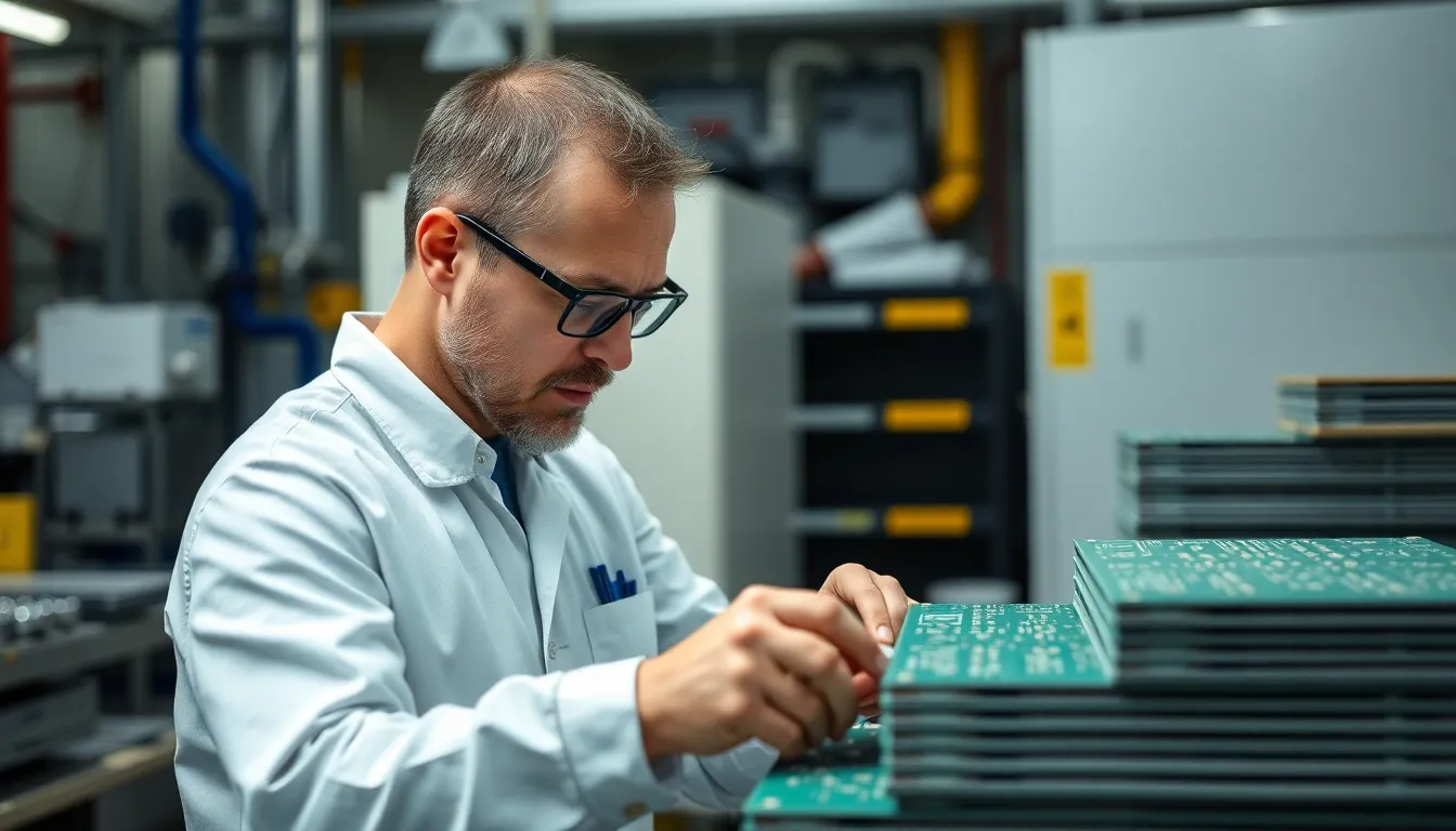
PCB panelisation plays a crucial role in efficient, cost-effective circuit board production at scale. Many designers question whether PCB manufacturers handle this critical process or if they must manage panelisation themselves. Understanding manufacturer responsibilities for panelisation helps streamline production workflows from design to finished product. Companies like https://www.wellpcb.com/ routinely manage panelisation services to optimise manufacturing compatibility and reduce per-unit costs for both prototype and large-scale orders.
Understanding PCB Panelization
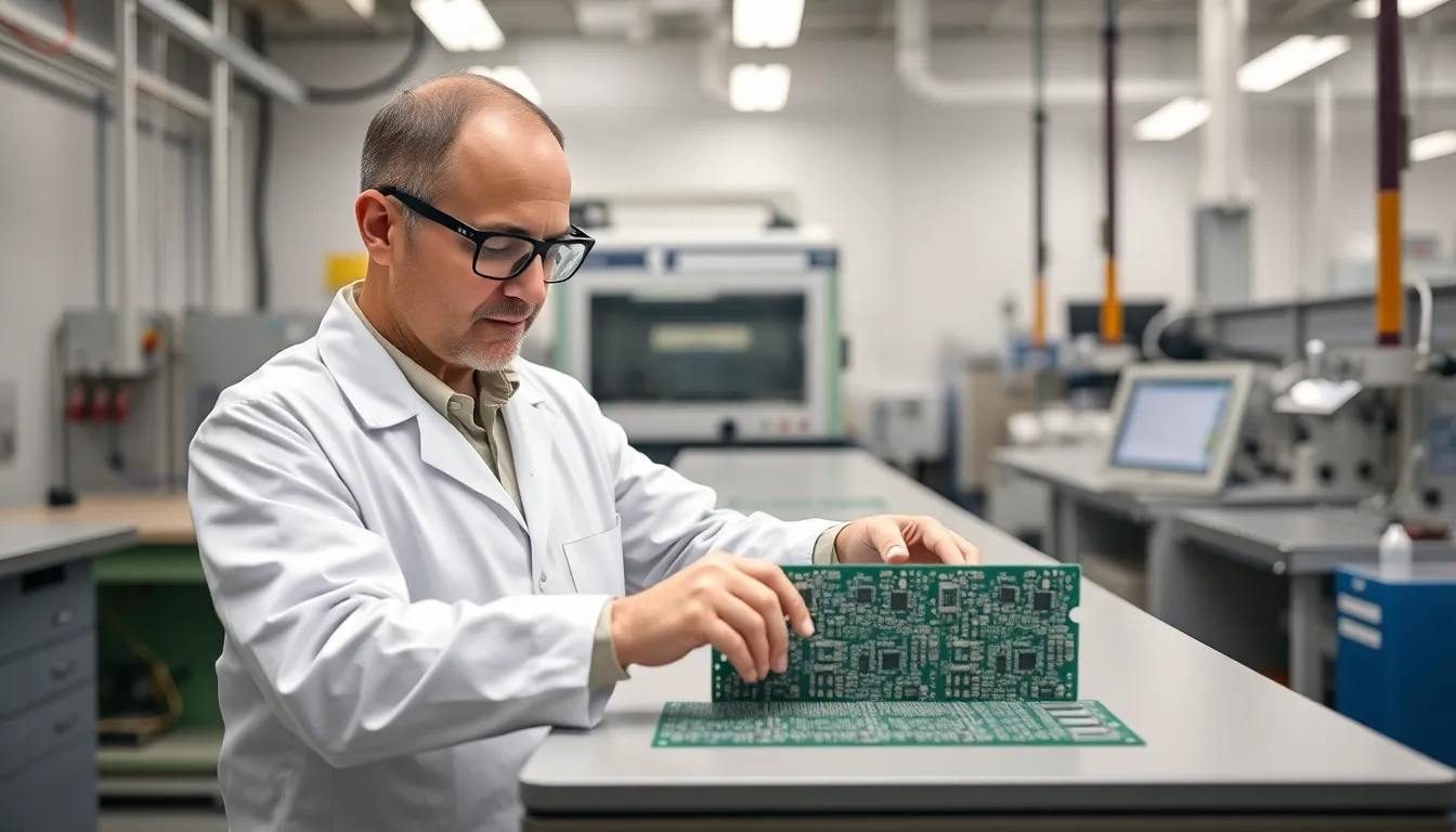
PCB panelization joins multiple board designs or copies into a single manufacturing panel for efficient processing, soldering, and assembly. Manufacturers like WellPCB use panelization to reduce waste, optimize production runs, and lower per-unit costs for clients producing prototypes or high-volume orders.
Designers supply either pre-panelized files or single board layouts. Manufacturers like WellPCB accept both options, but they often create custom panel layouts based on equipment size, order quantity, and depaneling method preferences.
Common panelization techniques include V-scoring for straight-line depaneling and tab-routing for complex outlines. Steps such as fiducial placement, breakaway tab location, and edge clearance get tailored to the specific assembly process. WellPCB applies international PCB standards and supports unique specifications from global electronics companies, ensuring each panel meets quality requirements.
Manufacturers communicate panelization decisions early in the ordering process and may suggest adjustments for yield improvement or assembly compatibility. They factor in solder mask spacing, component overhang, and board array orientation, especially for surface-mount technology (SMT) and automated assembly lines.
Why Panelization Matters in PCB Manufacturing
Panelization creates a unified array of PCB units, letting manufacturers like WellPCB process multiple boards together during fabrication and assembly. This improves throughput rates in surface-mount technology (SMT) and automated assembly lines, reducing production cycle times. Each panel maintains consistent spacing, which supports pick-and-place equipment accuracy for component mounting. Board designers and OEMs benefit from lower per-unit costs when manufacturers use panelized formats, as material usage becomes more efficient and manual handling decreases.
Uniform panel structures limit material waste, which is significant in high-volume orders handled at WellPCB’s facilities in China. Operators use predictable panel formats to streamline soldering and automated optical inspection (AOI). Efficient panelization also supports key assembly services such as selective depaneling and controlled stress distribution, preserving yield across board types including single-sided, double-sided, and multilayer PCBs.
WellPCB engineers adjust panel dimensions and tooling hole placements according to customer needs, factory equipment constraints, and international quality standards. They provide clients with feedback on fiducial placement for SMT registration and edge clearance for depaneling, contributing to success in global electronics production. Proper panelization planning preserves both functionality and structural integrity from initial batch runs to high-throughput manufacturing.
Do PCB Manufacturers Take Care of Panelization
PCB manufacturers, including WellPCB, regularly manage panelization for orders ranging from prototypes to large-scale production. This approach helps ensure the boards meet manufacturing requirements and simplifies downstream assembly.
Standard Panelization Practices
Standard panelization practices include placing multiple PCB units in a single array, creating tooling holes, and adding fiducials to support pick-and-place machinery. Most manufacturers like WellPCB use automation software to optimize panel layouts based on equipment specifications. Common depanelization methods include V-scoring, used for straight-line board separation, and tab-routing, used for irregular board shapes. Engineers configure edge clearance, orientation, and breakaway tabs according to IPC-2221 standards, adjusting dimensions to match each project’s requirements. Manufacturers, upon receiving single-board Gerber files, often provide feedback or create custom panel layouts to meet fabrication and assembly needs for both surface-mount and through-hole technologies.
Variations Across Manufacturers
Panelization procedures differ among PCB manufacturers due to factory capabilities, region, and order specifics. WellPCB builds custom panels for clients, considering board size, component clearance, and order volume to maximize material usage. Some manufacturers expect clients to provide panelized layouts, especially for complex multi-design panels, while others like WellPCB handle all panel setup with engineering support. Regional factories might set minimum order quantities or charge setup fees when creating custom panels for small batches. Equipment restrictions and assembly line configurations cause differences in breakaway tab spacing, v-score depth, and fiducial placement. Communication between the manufacturer and customer ensures each panel meets functional and structural requirements before mass production.
Factors Influencing Manufacturer Panelization Services
Manufacturer panelization services depend on customer orders, board complexity, and design requirements. WellPCB in China evaluates submission details to determine optimal panel layouts for consistent quality and efficiency.
Order Quantity and Complexity
Order quantity and PCB complexity affect manufacturer panelization services. Larger batch sizes, such as runs above 500 boards, require maximized panel utilization and efficient separation to reduce production cycle times. Smaller orders often use standard panel sizes, which limits the need for custom tooling. Complex designs needing mixed shapes, tight tolerances, or multiple layers increase planning and routing requirements. WellPCB adjusts slotting, tooling holes, and fiducial locations for high-density layouts or non-rectangular boards to match assembly line compatibility and automated processing. Edge cases, like rigid-flex PCBs or boards with heavy surface-mount assemblies, also affect panelization parameters to protect against warpage and improve depaneling yields.
Design Requirements and Customer Input
Design requirements and customer input influence manufacturer panelization services. Clients can submit single-unit designs or request custom panelization solutions for assembly compatibility or automated test needs. WellPCB collaborates with customers to align spacing, “mouse-bite” tab placement, and break-routing details for high-yield output, especially when the design uses nonstandard features or requires controlled impedance. Client specifications may include designated tooling hole positions, special fiducial marks, or requests for embedded test coupons. WellPCB’s team reviews submitted Gerber files, advises on necessary adjustments, and provides digital proofs of panel layouts for final approval, reducing production risks and supporting consistent global delivery standards.
Tips for Ensuring Proper Panelization
- Provide Clear Design Files
Designers ensure proper panelization by submitting Gerber files with layer details, board outline, and drill information. WellPCB‘s engineers use these files for custom panel layout and confirm compatibility with assembly equipment.
- Specify Panel Requirements Early
Specify requirements such as panel dimensions, array size, and routing method before production. For example, WellPCB adapts tooling hole placements, breakaway tabs, and fiducial marks based on project details at the quoting stage.
- Collaborate on Assembly Constraints
Communicate assembly constraints such as component overhang or pick-and-place locations. WellPCB reviews these constraints before setting V-scoring or tab-routing parameters for stencil and depaneling accuracy.
- Approve Digital Panel Proofs
Review and approve digital proofs of panelization layouts before mass production. WellPCB provides digital layouts for customer approval and addresses feedback on array orientation, part spacing, or edge clearance.
- Request IPC Standards Compliance
Ask for panelization solutions that meet IPC-2221 or IPC-7351 standards for board spacing and process compatibility. WellPCB’s standard panelization follows global IPC requirements for SMT, through-hole, and AOI processes.
- Review Feedback and Recommendations
Evaluate manufacturer feedback on fiducial placement, tooling hole locations, and breakaway configuration. WellPCB issues engineering change notices and improvement suggestions for higher yield and structural integrity.
- Document Special Panelization Needs
Record any non-standard panelization needs such as odd-shaped outlines or mix designs in a single panel. WellPCB supports mixed-board panels and complex array construction after confirming order specifics and testability requirements.
About WellPCB
WellPCB, located in Los Angeles, CA, is a leading provider of high-quality PCB manufacturing and assembly services.
Led by Hommer Zhao, Director of Sales and Marketing and Co-founder, WellPCB offers comprehensive solutions for PCB prototyping, assembly, and testing. The company is dedicated to delivering precision, reliability, and efficiency, ensuring that clients in industries such as electronics, telecommunications, automotive, and medical devices receive top-tier products and services.
Contact:
Hommer Zhao, Director of Sales and Marketing, Co-founder
Phone: (424) 842-2783
Email: [email protected]
Address: 3826 Medford St, Los Angeles, CA 90063, USA
Website: www.ourpcb.com
Frequently Asked Questions
What is PCB panelization?
PCB panelization is the process of grouping multiple printed circuit boards or designs into a single manufacturing panel. This allows manufacturers to fabricate and assemble multiple boards simultaneously, increasing efficiency and reducing production costs.
Who is responsible for panelization — the designer or the manufacturer?
Typically, PCB manufacturers handle the panelization process. Designers can submit either single board files or request specific panel layouts. Manufacturers use their expertise and equipment specifications to create the most efficient panel layout for each order.
How does panelization reduce costs in PCB production?
Panelization lowers costs by allowing multiple boards to be processed together, improving throughput and reducing material waste. This streamlines assembly and soldering processes, resulting in lower per-unit costs, especially for high-volume orders.
What are the common panelization techniques used in PCB manufacturing?
The two most common panelization techniques are V-scoring, which allows easy straight-line depaneling, and tab-routing, which is used for complex board shapes. Manufacturers may choose the best method based on board design and assembly requirements.
Can designers specify panelization requirements to manufacturers?
Yes, designers can specify panel requirements, such as spacing, board orientation, or special shapes. It’s important to communicate these needs early and review digital proofs provided by the manufacturer before the start of production.
Why is fiducial placement important in panelization?
Fiducials are reference markers that help automated machinery accurately place components during assembly. Proper placement ensures high-precision mounting and reduces the chances of assembly errors or misalignment.
What standards do manufacturers like WellPCB follow for panelization?
Manufacturers like WellPCB typically adhere to international standards such as IPC guidelines for panelization. These standards ensure proper board spacing, tooling hole placement, and process compatibility, meeting global quality and reliability requirements.
How does panelization affect the assembly process?
Panelization supports automated assembly by providing consistent spacing and alignment for pick-and-place machines, speeding up production, improving accuracy, and supporting efficient automated inspection processes like AOI.
What information should designers provide for optimal panelization?
Designers should submit clear and complete design files, outline desired panel requirements, and specify any special needs such as unique shapes or mixed designs. Early communication helps manufacturers optimize the panel for quality and assembly.
Is panelization necessary for both prototypes and mass production?
Yes, panelization is recommended for prototypes as well as mass production. It streamlines handling during fabrication and assembly for prototypes, and maximizes efficiency and yield for large-scale manufacturing orders.